[3/3] From the hardware to the cloud: Designing a PCB
In the previous article, I described the test carried out with the magnetic sensor MMC5883MA and explained the results obtained measuring the magnetic field with and without a vehicle's presence. However, before testing the other sensors (as I planned before), I decided to venture into a challenge which every hardware developer has to face at some point: to design and produce a Printed Circuit Board (PCB).
The breadboards are fundamental tools for hardware prototyping. They allow us to change and test the circuit design as many times as necessary, until having the best composition. In spite of that, these types of circuits are not intended to develop final products. The electrical connections provided by breadboards are temporary by nature, which means they are weak and unreliable. In addition, they tend to occupy more space than what they actually need.
By using PCBs, we are able to implement the final design of a hardware project with reliable connections and bigger robustness, besides reducing the space needed by allowing the use of smaller components, which are generally Surface-mount technology (SMT).
Today, there is a big variety of software made for PCB design. I decided to use Eagle, which is one of the most popular. The prototype to be implemented in the PCB is based on the circuit built in the previous article, designed to test the magnetic sensor MMC5883MA. Nonetheless, in this opportunity, I used the SODAQ ONE board instead of the NodeMCU ESP8266, with the objective of easily testing the magnetic sensor LSM303AGR, currently integrated on this board.
Furthermore, I had previously bought a surface-mount infrared sensor, with the IS31SE5000 reference, which I couldn't test before in the breadboard prototype due to its packaging. So I wanted to take advantage of this design and include the typical application circuit for this infrared sensor too, in order to be able to test its behavior and evaluate its capacity for vehicle detection.
In brief, for this stage of the project, I wanted to integrate the three mentioned sensors in a simple PCB and be able to transmit its measurements through LoRaWAN using the RN2903 module, also integrated on the SODAQ ONE board. Additionally, I found appropriate to add a power regulation stage to regulate the input voltage and protect the components.
Blocks diagram
It’s worth mentioning that the PCB is intended to use one sensor at a time. To achieve this, a "sensor selection logic" is added to the design, which consists of a single row male header with 6 pins and two jumpers, to select the SCL and SDA inputs for the I2C port of the SODAQ board. Also, a dip switch was added to disable the power from the unused sensor, in order to consume less power. The block diagram which describes the circuit composition is shown below.
The power regulation stage is based on the voltage regulator LM317T. The circuit was built with the help of the LM317's datasheet and configured to deliver of 3.3 V, the voltage needed for the SODAQ and sensors.
Eagle
Eagle is an Electronic Design Automation (EDA) software, powered by Autodesk, which provides useful and intuitive tools to design PCBs. Furthermore, it has a huge community worldwide, which implies that you can find documentation and examples easily, as well as answered questions.
A design in Eagle can be divided into two main parts: schematic, and PCB layout. Schematic is the part where the circuit components are selected and the connections between them are made. PCB layout refers to the distribution and physical placement of the components.
Before explaining how the schematic and the PCB layout for my project was made, it’s necessary to explain one of the most important concepts in Eagle design: the libraries.
Libraries
A library is the complete representation of an electronic component in Eagle. It contains all of its information, from the pin names to the physical measurements. If you want to use a component in an Eagle project, it's mandatory to have the library for that component. By default, Eagle includes a big amount of libraries of the most common components used in circuits. However, at some point, you could need a component which is not included. In this case, there are two options: looking for the component's library (there is a large variety on the internet thanks to Eagle’s community) or creating it by yourself.
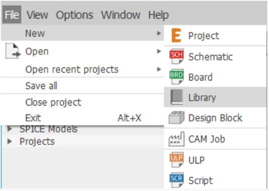
In my case, I needed to use three specific components which were not included in Eagle libraries: the two sensors and the SODAQ ONE board. Since I made some unsuccessful research, I decided to create them by myself. To create a library, you just need to go to the Eagle's Control Panel and click on the "File" menu, followed by "New" and then "Library”.
A new window will open. There you will find four spaces named Device, Footprint, 3D Package, and Symbol. The first step is to create a "Symbol", this is, the symbolic diagram which will represent the device in the schematic. To do this, click on the button "Add Symbol...", or the icon on the top marked with the "1" in the image below.
After that, it’s necessary to create a "Footprint", which corresponds to the representation of the physical device, and should have the precise dimensions of the component as well as the right distribution of the pins. This can be done by clicking the button "Add Footprint..." on the bottom, or the icon on the top marked as "2" on the image below.
The final step is to add a "Device". This element is a merge between the Symbol and the Footprint, where it must be specified which parts of the Symbol correspond to which physical part of the device. To do this, click on the button "Add Device..." or by clicking the icon on the top marked with the "3".
The preview of the results is shown on the right panel of the window. In my case, as the SODAQ board had male headers in its pins in order to be easily placed on a breadboard, the creation of the library for the SODAQ ONE was very simple because I only needed to add two female headers of 12 pins each (I wanted the SODAQ board to be removable). Something similar happened with the magnetic sensor, as I bought the evaluation board MMC5883MA-B, which has male headers too.
Nevertheless, the development of the library for the infrared sensor was very difficult for me because I had never worked with surface components. It is a very small component and I needed to be extremely accurate with the sizes and distances.
After a few hours of work, these were the resulting libraries.
- SODAQ ONE:
- Magnetic sensor (evaluation board) MMC5883MA-B:
- Infrared sensor IS31SE5000:
It’s important to note that the libraries created by the user can be found in the menu Libraries/libraries from the left panel of the Eagle's Control Panel.
Schematic
After having all the needed libraries ready, it's time to integrate the components in a schematic. To create a new schematic, go to the Eagle's Control Panel and click the menu "File", then "New" and after "Schematic".
In the schematic's window, to add a component go to the tools bar (generally on the left), use the tool "Add part" by clicking on the icon marked as "1" in the image below. To make the connections between the pins of the components, use the tool "Net" by clicking on the icon marked as "2".
After adding all the components of my design and making the respective connections, this was the outcome.
PCB
After having finished the schematic, the next step is to create a new "Board". To do this, click the icon "Generate/switch to board" on the top of the schematic's window (marked with the red square on the image below).
This will open a new window, where you will find all the components used in the schematic, with little lines joining them which represent the connections made in the schematic. Also, you will find a blank space which represents the physical board of the PCB. All the components have to be organized and distributed as best as possible on this blank space. Then, the little lines have to be converted into routes, which are the physical connections between the components in the PCB. To route the circuit is necessary to use the "Route Airwire" tool, which can be found in the left panel.
It’s important to mention that routing can be done in one or several layers. In addition, There are a lot of parameters that have to be kept in mind when you're in this stage of the PCB design. Some of them are: the thickness of the routes, the minimum distance between components, the minimum distance between consecutive routes, the width of the holes, etc. All of these design parameters must be supported by the PCB manufacturer you choose. Last but not least, you need to be very careful with the layer you're using.
After a few hours of more work, I achieved my objective of routing all my components in one layer. As I was working with one superficial component, I had to put it on the same layer of the routes. This was the result.
Gerber files
The final step to produce a PCB is to send the design to be manufactured. Although it is also possible to print the circuit by yourself, in this case I wanted to do it more professionally, so I looked for local manufacturers. To be able to send your design you need to generate the Gerber files of your circuit. To learn how to do it, I followed this tutorial. After having exported the corresponding files, I sent them to the manufacturer.
A few days later I received six copies of my PCB. I have to admit I was very excited to see that what I created was coming slowly to life. Honestly, these advances are the ones that could motivate you the most when doing a hardware project from scratch.
I was eager to prove if my design was correct, and if whether or not the circuit would work. So, without more delays, I started to solder all the components. Unfortunately, when I was about to solder the infrared sensor (the most difficult part), I realized I committed a mistake with the Footprint: the pins was inverted. I was concerned about my error but I knew that this first experience with surfaced components would help me a lot in future designs. This is how the PCB looked when I finished soldering the components.
Finally, I was ready to test the rest of the circuit. So I added a battery and turned on my LoRaWAN gateway. After a few seconds, I was receiving data of the magnetic field measurements in my Ubidots account! This meant that the behavior of the PCB was as expected.
The PCB design is a wide world where the techniques, software, and tools are enhanced every day. In this article, I tried to describe the basic process to take your circuit from the prototype to the PCB, but there is a long way to explore yet. I hope my experience can become a guide for those who are starting. However, the most important thing is to not give up at the first mistake, and don't stop exploring and improving your abilities to produce better and better circuits.
Keep attentive to the next posts to know the rest of the process!